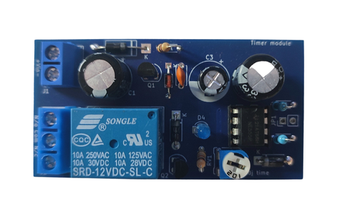
555 Timer Project
Difficulty rating: Beginner
Average time to build: 30 minutes
The 555 IC is a great choice when building timing circuits. The 555 IC is probably the most useful IC to play with when you learn about electronics.
Short description
This DIY kit will help with your soldering skills, while you learn about the standard 555 timer IC.
The kit learns you how the IC can be used to get a set time for powering the relay ON.
It intergrades a voltage-follower NPN transistor and Zenner as a stable voltage regulator.
So you can power it with a wide voltage range and no need to worry about the timing varying between the on-off times of the Relay.
555 Timer building summary
In this project, you will need the kit as well as a soldering iron, solder and pliers to cut the legs of the components shorter once completed
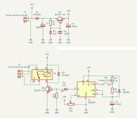
Project diagram
How the 555 Timer works
The IC 555 timer is a chip used in various areas and applications like pulse generation, an oscillator, and a timer. The 555 Timer is designed using 25 transistors, 2 diodes and 15 resistors.
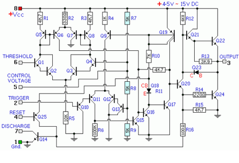
Fig: 555 Timer IC Internal Circuit
The functional parts of the 555 timer IC include a flip-flop, voltage divider & a comparator altogether. The main function of this IC is to generate an accurate timing pulse for operating various devices and electronic components.
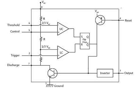
Fig: 555 Timer IC Block Diagram
The voltage divider consists of three 5k resistors which create two reference voltages. The reference voltages are 1/3 and 2/3 of the supplied voltage that ranges from 5 to 15V.
Then, two comparators compare two analogue voltages. If the input voltage at the positive terminal is higher than the input voltage at the negative terminal the comparator will output 1. Similarly, if the voltage at the negative input terminal is higher than the voltage at the positive terminal, the comparator will output 0.
The first comparator -ve input terminal is connected to the 2/3 reference voltage at the voltage divider and the external control pin, while the +ve input terminal is to the external Threshold pin. The second comparator -ve input terminal is connected to the Trigger pin, while the +ve input terminal is to the 1/3 reference voltage at the voltage divider.
So using the three pins Trigger, Threshold & Control, we can control the output of the two comparators. The output is then fed to the R and S inputs of the flip-flop. The flip-flop will output 1 when R is 0 and S is 1 or vice versa. The flip-flop can be reset via the external pin called Reset which can override the two inputs, thus resetting the entire timer at any time.
The Q-bar output of the flip-flip goes to the output stage or the output drivers which can either source or sink a current of 200mA to the load. The output of the flip-flop is also connected to a transistor that connects the Discharge pin to the ground.
555 Timer IC Pinout
The 555 Timer IC has 8 Pins which are explained below in detail.
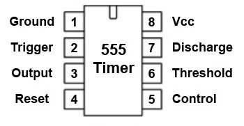
Pin 1: GND Pin
Ground pin directly connected to the negative terminal of the power source. It is suggested that it should not be connected using any resistor because all the IC will heat up due to stray voltage (it is the occurrence of electrical potential between any two objects that ideally should not have any voltage difference between them at all) in it.
Pin 2: Trigger Pin
A trigger pin is used to activate the IC’s timing cycle for operating. It is a low signal pin and the timer is triggered when the voltage is below one-third of the supply voltage (1/3 V). It is connected to the Inverting input of the comparator inside the IC and accepts negative signals for the operation.
Pin 3: Output Pin
It is the output pin. As the IC is triggered the output pin goes high depending on the duration of the timing cycle provided to it. In the case of logic zero o/p; it is a sinking current with a voltage greater than zero (0 V). Whereas, in the case of logic high output, it is sourcing current with the output voltage lesser than Vcc.
Pin 4: Reset Pin
The reset pin is used to reset. It should be connected to the positive terminal to work the IC properly. If this pin is grounded, the IC won’t work at all. The required reset voltage is 0.7 volts at a current rating of 0.1mA to work.
Pin 5: Control Voltage
It is used for reliable operation. When not in use, it should be connected to the ground through a capacitor; otherwise, the IC will show erratic responses (deviating from the desired value).
Pin 6: Threshold Pin
It detects when the voltage on the timing capacitor rises above 0.66Vcc. The timing cycle is only completed when the voltage on this particular pin is equal to or greater than 2/3 of Vcc.
Pin 7: Discharge pin
It is used to provide a discharge path from the timing capacitor to the ground when the output is low. The discharging current should be less than 50 mA to prevent it from being damaged.
Pin 8: Supply Terminal
It is a positive (+ve) terminal that is connected to the positive terminal of the power supply to power up. It is used to take power supply voltage from the power source for operation.
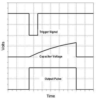
MONO-STABLE MODE
In the mono-stable mode, the circuit generates only a single pulse when the timer gets Powered. Pulse duration usually depends on the resistor and capacitor values and can be adjusted with RV1 (pot) to get the time for the relay to stay ON.
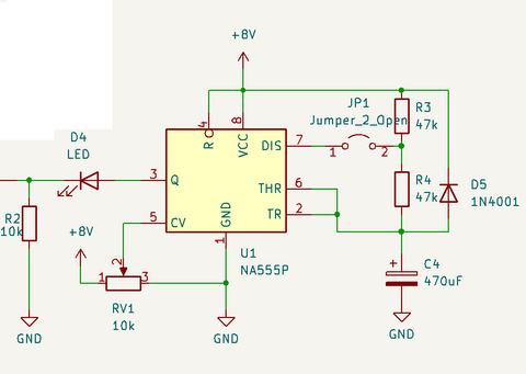
If we applied power to the circuit, then the capacitor gets charged and the timer circuit extends a high pulse, then it remains high until the THR is retched and output will go LOW and wait till power is disconnected and the capacitor gets discharged by D5. If it is necessary to enhance the time delay, then a higher rate of capacitor and resistor are required as necessary.
Step-by-step instructions.
The picture above shows all the components that come with the kit.
Step1
Place all Resistors, Diode, Zenner and solder pins (always start with the lowest components, this will make soldering easy when flipping PCB when soldering bottom.)

Step2.
Place IC holder, ceramic Cap and solder pins(these are the next higher components.)

Step 3.
Place 10k pot and 2Pin with 3Pin connector and solder pins (this will be the next highest components.)

Step 4
Place Electrolytic Capacitors and make sure of polarity they do have +,- pins neg are marked with white marking on the side and short wire pin, and last place the Tip120 NPN transistor with a metal case to the back as seen in the picture and Mosfet next to it and solder pins.

Step5
Finally, we can inspect the board for any shorts or missing soldering pins.
If all looks good we can power the board and we will test the Timer.
555 Timer Kit