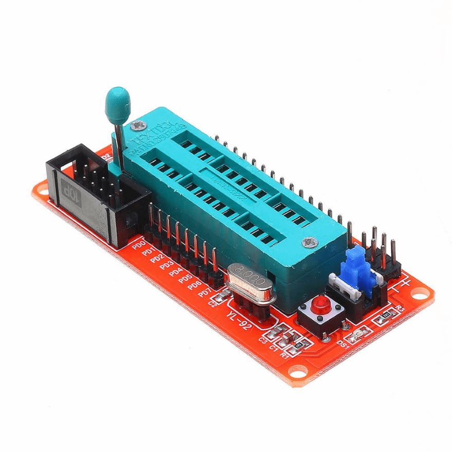
AVR Microcontroller Minimum System Board ATmega8 Development Board
Ever battled to program an Atmega8? By using this breakout board with a socket, you can easily place your IC in the socket to make connections to all necessary pins, you can then program the IC by connecting the board our ISP (In Circuit Programmer).
VCC Digital supply voltage 5Vdc max.
GND Ground.
Port B (PB7..PB0)
XTAL1/XTAL2/TOSC1/TOSC2
Port B is an 8-bit bi-directional I/O port with internal pull-up resistors (selected for each bit) Port B output buffers have symmetrical drive characteristics with both high sink and source capability. As inputs, Port B pins that are externally pulled low will source current if the pull-up resistors are activated. The Port B pins are tri-stated when a reset condition becomes active, even if the clock is not running. Depending on the clock selection fuse settings, PB6 can be used as input to the inverting Oscillator
amplifier and input to the internal clock operating circuit.
Depending on the clock selection fuse settings, PB7 can be used as output from the inverting Oscillator amplifier. If the Internal Calibrated RC Oscillator is used as a chip clock source, PB7..6 is used as TOSC2..1 input for the Asynchronous Timer/Counter2 if the AS2 bit in ASSR is set.
Port C (PC5..PC0) Port C is a 7-bit bi-directional I/O port with internal pull-up resistors (selected for each bit).
Port C output buffers have symmetrical drive characteristics with both high sink and source capability. As inputs, Port C pins that are externally pulled low will source current if the pull-up resistors are activated. The Port C pins are tri-stated when a reset condition becomes active, even if the clock is not running.
PC6/RESET If the RSTDISBL Fuse is programmed, PC6 is used as an I/O pin. Note that the electrical characteristics of PC6 differ from those of the other pins of Port C.
If the RSTDISBL Fuse is unprogrammed, PC6 is used as a Reset input. A low level on this pin for longer than the minimum pulse length will generate a Reset, even if the clock is not running. The minimum pulse length is given in Table 15 on page 38. Shorter pulses are not guaranteed to generate a Reset.
Port D (PD7..PD0) Port D is an 8-bit bi-directional I/O port with internal pull-up resistors (selected for each bit).
Port D output buffers have symmetrical drive characteristics with both high sink and source capability. As inputs, Port D pins that are externally pulled low will source current if the pull-up resistors are activated. The Port D pins are tri-stated when a reset condition becomes active, even if the clock is not running. Port D also serves the functions of various special features of the ATmega8.
RESET Reset input. A low level on this pin for longer than the minimum pulse length will generate a reset, even if the clock is not running. Shorter pulses are not guaranteed to generate a reset.

Another view of the atmega8 pin diagram
Technical Specifications:
- 23 IO pin all the leads.
- Classic ATmega8 minimum system, eliminating the hassle of soldering
- Crystal: The socket hole welding facilitate the buyer to replace the crystal, default 8MHZ crystal
- Support chip: ATmega8
- Power supply: ISP downloader or external expansion pin power supply (max 5V).
- External expansion 3 channel VCC, GND, as shown in the pin (max 5V).
- Reset: Power-on reset and reset button
- external expansion 4 led lights for easy debugging
- Power LED (DS1)
- Standard ISP download interface, by using 51/avr Downloader could easily download the program to achieve minimum system programming (the board does not require a separate power supply, support ISP download interface power supply)